Datasheet4U.com - GS816218DGD-250

GS816218DGD-250 Datasheet, GSI Technology

GS816218DGD-250 Datasheet, GSI Technology

Page 1 of GS816218DGD-250 Page 2 of GS816218DGD-250 Page 3 of GS816218DGD-250

GS816218DGD-250 srams equivalent

  • 18mb s/dcd sync burst srams.
  • Preview is limited to up to three pages.

GS816218DGD-250 Features and benefits

GS816218DGD-250 Features and benefits


* FT pin for user-configurable flow through or pipeline operation
* Single/Dual Cycle Deselect selectable
* IEEE 1149.1 JTAG-compatible Boundary Scan
* ZQ.

GS816218DGD-250 Application

GS816218DGD-250 Application


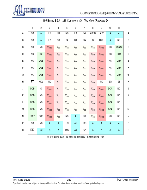
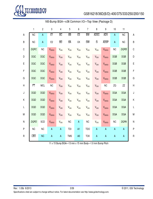
* JEDEC-standard 119-bump and 165-bump BGA packages
* RoHS-compliant packages available Functional Description A.

GS816218DGD-250 Description

GS816218DGD-250 Description

Applications The GS816218/36D is an 18,874,368.

Image gallery

Page 1 of GS816218DGD-250 Page 2 of GS816218DGD-250 Page 3 of GS816218DGD-250

TAGS

GS816218DGD-250
18Mb
DCD
Sync
Burst
SRAMs
GSI Technology

Manufacturer


GSI Technology

Related datasheet

GS816218DGD-200

GS816218DGD-150

GS816218DGD-333

GS816218DGD-375

GS816218DGD-400

GS816218DGD-xxxV

GS816218DGB-150

GS816218DGB-200

GS816218DGB-250

GS816218DGB-333

Since 2006. D4U Semicon.   |   Datasheet4U.com   |   Contact Us   |   Privacy Policy   |   Purchase of parts